Table of Contents
gEDA
Installation
– For Debian the installation is very easy
aptitude install geda-gschem geda-symbols geda-utils geda-gnetlist pcb geda-xgsch2pcb git
- After installation, copy your library folder into your “home directory”.
- Create the .gEDA directory in your home if it does not yet exist
- Create ~/.gEDA/gschemrc
Configuration
At bolay.co, we use our internal library. We didn't need to install them system wide. We prefere to add the library for each project as a git sub-module, referring to the exact version of library that match this project.
Create a new project
- Create a new directory for the project
- Init a git repository
- Clone the gEda_Library repos to Libs (With git submodule)
- Copy gitignore from Libs/Config/gitignore to .gitignore
- Launch install script (./Libs/install.sh)
  mkdir ~/Projects
  cd ~/Projects
  mkdir mynewproject
  cd mynewproject
  git init
  git submodule init
  git submodule add git@git.bolay.co:gEDA_library.git Libs
  cp Libs/Config/gitignore .gitignore
  ./Libs/install.sh
When cloning a project from git.bolay.co, don't forget to do:
  git clone git@git.bolay.co:MyProject.git
  git submodule init
  git submodule update

  git pull origin <branch>
Or
  git clone --rerursive git@git.bolay.co:MyProject.git
  cd MyProject
  git pull origin <branch>
When you want to modify a libray:
  ./Libs/install.sh
  cd Libs/
  git checkout origin/develop # Don't forget

  # Do something
  git commit -am "Message like Add DS18B20.sym"
  git push # Don't forget
  cd ..
  git commit -am "Update gEda Library"
Create Symbol
- Open “gschem” (Editeur de schémas gEDA)
- Select the board with the mouse and click “delete”
- Add → Pin (Rename it whit a correct name)
- Add → Box
- With this “options” you can create which symbol you want
- “Right Click” on the grill → Add atribute → Select footprint(boîtier), device (Description) and refdes (U?,D?,Q?) to give a name
- Select all the component : Edit → Symbol translate → The number is 0 because it's an original component
- File → Save as → el3/library/gschem-sym/… (Rename it COMPONENT.sym)
- Close gschem
- Your component is created
Attributes on Schematic
- device = The name of the symbol (BC337, 1N4148, TMLM0424)
- refdes = Abreviation of the component like : R (Resistor), U (Integraded circuit)…
| Prefix | Component type |
|---|---|
| R | Resistor |
| RN | Resistor Network |
| FB | Ferrite Bead |
| L | Inductor |
| C | Capacitor |
| B | Battery |
| F | Fuse |
| J | Connector |
| P | Connector (usually plugs that mate with J<n>) |
| K | Relay |
| S | Switch |
| T | Transformer |
| TP | Testpoint |
| M | Motor |
| D | Diode |
| Q | Transistor |
| U | Integrated circuits |
| X | Crystal (Quartz) |
- value = The value of your component : 1k, 5V,
- footprint = The footprint of your component (1206, SOT23, SOD-80)
- graphical = The component who has Graphical = 1 is ignored from gnetlist. A component who isn't eletrical like a box is configured like this.
- description = It's a description who representing the component (4 door nand with 2 input)
- slot = This attribute is used to specify a slot for a slotted component.
- net = The net attribute is used to create power/ground and arbitrary nets.
- netname = This attribute is used to know to which net your pin is connected.
- symversion = The symversion attribute is used to version the contents of symbols.
- comment = This attribute is used to supplementary commentary who can be useful for the component
- author = It identified the creator of the symbol (Name and adresse mail)
- numslots = Use for component who have many component into him. Like 74HC00 = 4 Nand into this component : Numslots = 4
- slotdef = In a 74HC00 there's 4 NAND with 2 inputs. (2 input → 1 output) Slotdef is one part of four from the 74HC00 : Slotdef = 1 : 1,2,3 ; Slotdef = 2 : 4,5,6 ; Slotdef = 3 : 7,8,9 ; Slotdef = 4 : 10,11,12
- documentation = This attribute is the documentation (datasheet) from the component in file oder URL. (documentation = 74HC00.pdf ; documentation = http://www.datasheetcatalog-74HC00.pdf) you can open the datasheet with : Hierarchy → Documentation
- source = this attribute is used when a symbol was created in a another schematic : source = NiX1-V1-CON.sch
- pintype = This attribute is used to give a specifical type for a pin (pintype = clk…) :
| Prefix | Name |
|---|---|
| in | Input |
| out | Output |
| io | Input/Output |
| oc | Open collector |
| oe | Open emitter |
| pas | Passive |
| tp | Totem pole |
| tri | Tristate (High impedance) |
| clk | Clock |
| pwr | Power/Ground |
Then, this attribute will be used from the DRC and netlisting.
- pinseq =
- pinlabel = It's an logic text for the label. In an ampliop : IN+, IN-, Output, VCC, -VCC.
- pinnumber = Every label has a number, the reference is in the datasheet. (pinnumber = 7)
- dist-license = The dist-license attribute is used to specify the redistribution license for the symbol or schematic. It should be the name of a known license. Some examples values are: GPL, GPL version 2 only, GPL version 3 only, public domain, Apache version 2, Modified BSD, X11, etc. For a list of licenses see : FSF License List and OSI License List.
- use-license = The use-license attribute is used to specify the license for how the symbol or schematic can be used by another people in her circuits.
Add and edit attributes via Gattribs
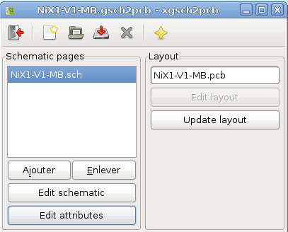
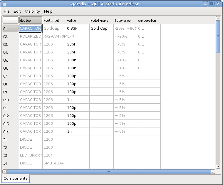
With geda it's too easily to edit or add attributes. First you open your gsch2pcb and add the schematic. Then you click on edit attributes.
Now you can edit, add and delete attributes with the “Edit” Options in the top of the program. If you want to the attributes be invisible in the schematic, use the “Visibility” options. It's too easily too understand.
- Visibility → Set selected invisible : Your attributes will be invisible
- Visibility → Set selected name visible only : Only the name of the attributes will be visible (Device, footprint,refdes)
- Visibility → Set selected value visible only : Only the value of the attributes will be visible (BC337, SIP-8,D1)
- Visibility → Set selected name and value visible only : The name and value of your attributes will be visible
Change title block at start up
- Open the terminal and write :
el3@bolay:~$ vim ~/.gEDA/gschemrc
- press i (insertion mode)
- Add or modify this line
(define default-titleblock “Name_of_your_Titleblock.sym”)
- press :wq
Refdes automatically numbered
- Open the terminal and write :
el3@bolay:~$ vim ~/.gEDA/gschemrc
- press i (insertion mode)
- Add or modify this line
Note: Starting with version 1.2 of gschem the name of the path variable has changed:
- (load (string-append geda-data-path “/scheme/auto-uref.scm”)) = load the autonumbering script
- (add-hook! add-component-hook auto-uref) = autonumber when adding a component
- (add-hook! copy-component-hook auto-uref) = autonumber when copying a component
Create Footprint
- Open “PCB Designer”
- Select the “impression” face
- Create the component with line, arc and vias
- When you do a line : at the top right of your program you can see the longer of your line
- To give a name to your vias select him and use “n” and rename it
- Your component is finish ?
- Select all the component : Select → Convert the selection on element (Convertir la sélection en élement)
- Click on a pin or on the component
- Buffer → Cut the selection on tampon (Couper la sélection dans le tampon)
- Buffer → Save the element of the tampon on a file (Sauvegarder les élements du tampons dans un fichier)
- Your component must be save at el3/library/pcb-elements/…
- File → Save as el3/library/pcb-elements/…
- You have two copies of the component
- Your component is created
- Use “s” to make the vias thick (grand, épais)
- To enlarge a page : File → Preference → tailles
- To be precise with your line : view → grid size → 1 mil (Be careful the unit at the top right of your program is now in mil click on him to change to mm)
First create your component, you can use the circle to be faster and create the “big pad”.
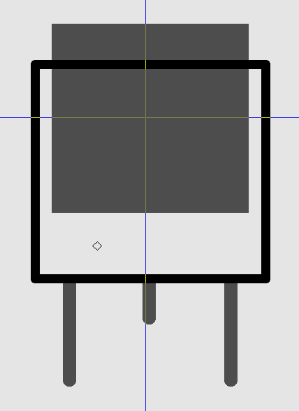 Select your component and : Select → Convert the selection on element. Then you can modify the file with gedit to have the pad rectangular :
Element["" "" "" "" 100079 67850 0 0 0 100 ""]
Pad[8316 160 15718 160 4000 2000 6000 "" "2" "square"]
Pad[-16731 167 -9329 167 4000 2000 6000 "" "1" "square"]
ElementLine [-16851 14276 -14646 16481 1000]
ElementLine [-16850 -13992 -14646 -16196 1000]
ElementLine [15827 -16196 15827 16481 1000]
ElementLine [15827 16481 -14646 16481 1000]
ElementLine [-16851 14276 -16851 -13992 1000]
ElementLine [-14646 -16196 15827 -16196 1000]
With “square” your pad will be rectangular. The modification has made with gedit.
For more information, please visit : http://www.brorson.com/gEDA/land_patterns_20070818.pdf or another link for the same doc https://github.com/evanfarrar/opensprints/raw/0b994c2b6b539b8a3beab4ea42a6447f10e396a3/hardware/interface_board/geda/docs/land_patterns_20070818.pdf
Schematic to PCB
- Open gschem and create your schematic
- When your schematic is finished save it at a new folder
- Close the program
- Make a “Liens symbolic” :
- Open the terminal
- cd /AAA/BBB/NAME_OF_REPERTORIES
- ln -s /home/el3/library/PCB-elements packages (PACKAGES MUST BE AT THE END)
- You have create a “Liens symbolic”
- Cf : Chapter : Add libraries to a single PCB project
- Click right on your schematic and open with “gEDA Schematic to PCB Project”
- Add your schematic and click update layout
- If there is an footprint error you have make an error
- If there isn't any error, you can start your PCB.
If the first solution does not work, try this:
- Open the terminal
- cd /AAA/BBB/YOUR_FOLDER (Folder where your schematic is located)
- gsch2pcb -d /AAA/BBB/YOUR_SCHEMATIC.sch
- Now, a new file was created on your folder (YOUR_SCHEMATIC.pcb)
- Run the .pcb and it's done
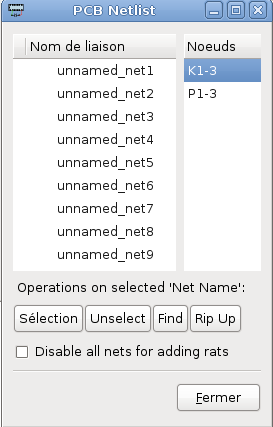
Sometimes, the netlist does not load:
- In the .pcb, select File→Load netlist file
- Search in your folder the .net
- Type o to optimise rat
- You can start route
Import the board on PCB
- Open the model with “gedit”
- Copy the layer 8 for the board :
Layer(8 “outline”)
(
Line[229994 203220 229994 33927 800 0 ""]
Line[35059 228756 204404 228810 800 0 ""]
Line[35112 8338 204404 8337 800 0 ""]
Line[204404 8337 229994 33927 800 0 ""]
Line[204404 228810 229994 203220 800 0 ""]
Line[9522 33928 9522 203219 800 0 ""]
Line[9522 203219 35059 228756 800 0 ""]
Line[9522 33928 35112 8338 800 0 ""]
)
- Now open your pcb with “gedit” and paste that instead layer 8
- Save that and open and the board is on your PCB !
- You can too copy the layer 9 for the text for example
Documentation
On debian you can read a lot of useful information directly from the installation doc files.
/usr/share/doc/pcb-common/
.
├── changelog.Debian.gz
├── changelog.gz
├── copyright
├── examples
│   ├── LED
│   ├── LED2
│   ├── LED.NET
│   ├── libraries
│   │   ├── example.inc
│   │   ├── example.list
│   │   └── example.m4
│   └── tut1.pcb
├── NEWS.gz
├── pad.png
├── pcb.html
├── pcb.pdf.gz
├── puller.png
├── refcard.dvi.gz
├── thermal.png
└── Whats_new_in_2.0.gz
Here you can especially read pcb.pdf.gz. And you can also print this useful refcard
Add libraries to a single PCB project
To add PCB components to your project use the following method to add a folder to your libraries :
- Open a terminal
- use the cd command line to access your project directory
- Once you are in your projet's directory, use the “ln -s” command to link a folder as library to your project
- Now open or re-open your project and all components must have been added to your library
In the following example, our project is in : ~/home/dzuf/pcb_project/project_test
and our folder path is : ~/home/dzuf/pcb_library
So, we open a terminal and write the following lines :
1.
cd /home/dzuf/pcb_project/project_test
2.
ln -s ../../pcb_library packages
Now the folder “pcb_library” has been added to our project library
Verifying your symbols
Before using a symbol in geda, it may be useful to check if there aren't any error. Run gsymcheck -vv over the symbol you want to control.
gsymcheck -vv component_name.sym
If any errors occures, you can correct them directly by using the terminal.
- Move to the component directory with terminal
- Then use the vi text editor over the symbol
vi component_name.sym
Pin types
In gEDA, there are pre-defined pin types, so be sure to use them, otherwise gsymcheck won't accept them.
You'll find those types by following the link “geda attributes”, then go to page 7.
Sending components to the bottom of the board
To send single component to the bottom of the board :
- Put your mouse over the component to send, and press the “b” key
To send multiples components to the bottom :
- Select the components you want to send to the bottom
- Press the “maj+b” key
Send tracks to another layer
To send one single track segment to another layer, select the layer, then with the mouse over your track's segement, press the “m” key.
To send multiple track's segements to another layer, select the layer, select the segments, then press “shift+m”.
Edit a component
Open your component file with PCB Designer. Select all your component, copy it into the buffer with “ctrl+c” or “ctrl+x”. Select Buffer in the toolbar, click to Break buffer elements to pieces and Paste buffer to layout or “ctrl+v”. Now you can edit your component. Don't forget to give a name to all pad with “n”.
If you want to convert your component into a single element, select all your component , copy it into the buffer. Select Buffer in the toolbar, click to Convert buffer to element and Paste buffer to layout. It's done, your component is edit.
Add a new footprint in your pcb
- Open the terminal
- cd /AAA/BBB/YOUR_FOLDER (Folder where your schematic is located)
- gsch2pcb -d /AAA/BBB/YOUR_SCHEMATIC.sch
- Run pcb on your file YOUR_SCHEMATIC.pcb
- Select File → Load layout data to paste buffer
- Select YOUR_SCHEMATIC.new.pcb to load your new footprint
- Select File → Load netlist file and select YOUR_SCHEMATIC.net
- Type o to optimize rat
PCB Tips
While routing your PCB, you may win some time by using the predefined hot-keys from PCB :
- F1 ⇒ Via tool
- F2 ⇒ Routing tool
- F3 ⇒ Arc tool
- F4 ⇒ Text tool
- F5 ⇒ Rectangle tool
- F6 ⇒ Polygon tool
- F7 ⇒ Buffer tool
- F8 ⇒ Delete tool
- F9 ⇒ Rotate tool
- F11 ⇒ Selection tool
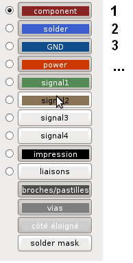
While routing, if you want to change layer, simply press the number associated to the layer. They are ranked from the top to the bottom :
If you want to replace the “REFDES” on PCB, you must click on nothing (Where there isn't any coamponent), press “f” and then take the “REFDES” with the mouse and you can place it where you wnt.
There's some useless keyboard shortcut on gEDA :
- 1 to 9 ⇒ change layer
- F1 to F11 ⇒ Tool selection (all description in PCB Tips)
- del ⇒ delete component, track, via, etc at the cursor location
- shift+del ⇒ delete selected objects
- u ⇒ undo operation
- shift+r ⇒ redo operation
- m ⇒ move our track on the selected layer
- shift+m ⇒ move selected object on the selected layer
- b ⇒ change a component between the top and the bottom
- shift+b ⇒ change all component selected between the top and the bottom
- z & shift+z ⇒ Zoom
- v ⇒ zoom out completely
- tab ⇒ switch the side of the view
- n ⇒ edit all kind of text
- h ⇒ show/hide component name
- d ⇒ show/hide the number/name of pin/via
- f ⇒ highlight selected connection
- shift+f ⇒ reset all highlight connection
- i ⇒ open library window
- : ⇒ open user command
- s & shift+s ⇒ change the width of lines, arcs, text objects, pins,pads and vias at the cursor location
- l & shift+l ⇒ change the width of our track while routing
- / ⇒change the routing style: none, _ /, \ _
- g & maj+g ⇒ add or subtract 5mils to the grid
- ctrl+g & maj+ctrl+g ⇒ add or subract 0.05mm to the grid
- maj+v & maj+ctrl+v ⇒add or subtract 5mil to default via size
- alt+v & maj+alt+v ⇒add or subtract 5mil to default via drill
- o ⇒ acualise and optimize all rats
- q ⇒ make a line/pad rectangular
- k ⇒ increase the size of the clearance of a track
- shift+k ⇒ decrease the size of the clearance of a track
Plan de masse
Pour pouvoir créer un plan de masse ou de VCC, il suffit de tracer un rectangle.
En utilisant l'outil THRM et en cliquant sur des trous, cela va directement connecter le trou au plan.
Pour connecter directement une piste au plan, il faut décocher la case “New lines, arcs clear polygons” dans l'onglet Settings. Ainsi, lorsqu'on tracera une nouvelle piste, elle va se connecter toute seule au plan. Pour les anciennes pistes, il faudra les retracer, autrement elles ne seront pas connectées.
Attention: cochez à nouveau la case si vous refaites une piste qui ne doit pas être connectée au plan !
Create a build of material from shematics
Open the terminal and write this command :
- cd /Document_of_your_project : Go to the document of your project
- ls : verify your file in the document
- touch attribs : create a file
- gnetlist -g bom -o bom.txt NiX1-V1-MB.sch the first bom (build of material) is a command and the second is the name of your file
- touch bom.txt : Create the txt file
- cat bom.txt : see a preview of bom.txt
- cat attribs : see which attribs you have added
- vi attribs : then press i to go in insertion mode
- and write the “options” you want to add at your build of material. (value, footprint) Refdes is automatically added.
- when you finish presse enter, ESC and write :wq use to get out of vi attribs
- gnetlist -g bom -o bom.txt NiX1-V1-MB.sch (actualize the file)
- Your build of material is created
Create a PS Schematic
- Open the terminal
- cd home/el3/NiX1/Folder of your project
- $ gschem -v -p -o Name_of_file.ps -s /usr/share/gEDA/scheme/print.scm Name_of_your_schematic.sch
- Your file is created in the folder who the project is
Create a .zip with the terminal
- Open your terminal
- cd /Projectfile
- $ 7z a -tzip Projectfile.zip .
Create a screen of your PCB
To create a screen and print it, you must export the layer :
File → Export layout → PNG
Check the “as-shown” options and write 1000 to the DIP. (Pixel)
Simulation with Gnucap and Gwave
With gnucap you can “export” your schematic and do a simulation. But you must add a netname to your connection. For example :
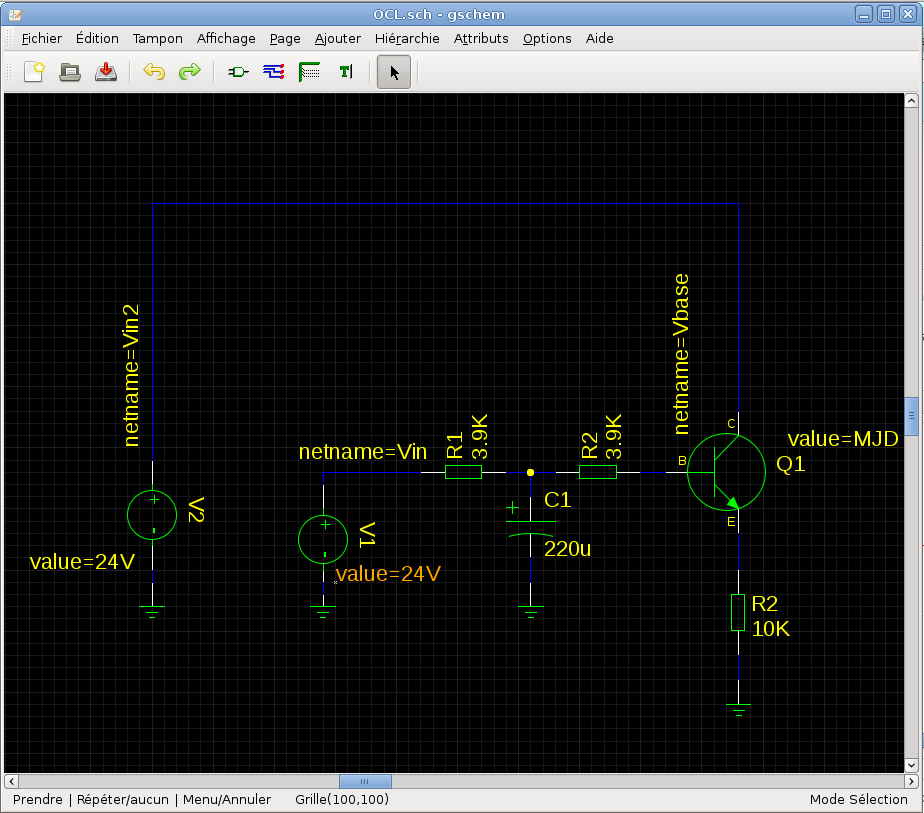 Here you can see we have add the netname attribute for some connections, the value attribute for the transistor and the voltage source are useful.
When your schematic is finish, open the terminal :
- ~cd /file of your project
- ~gnetlist -g spice -o netlist-of-your-shematic.net your-schematic.sch
- ~gnucap
- You enter in the options of gnucap
Important : “build” is used to modify or add for example an voltage source, “list” is used to see all your component, Links :
There's three very important links to understand how to use Gnucap.
You can use a script to be faster with Gnucap. Write on gedit the command you want use in the options of Gnucap. For example :
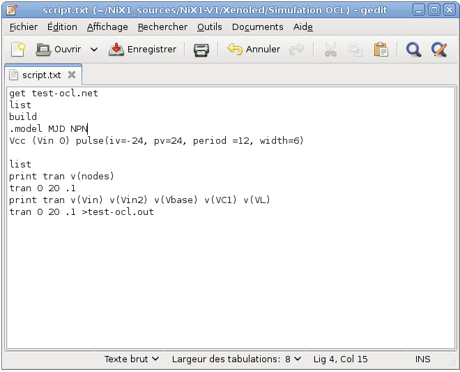 That must be saved in the same folder of your project.
Then open your terminal :
- ~ cd /file of your project
- ~ gnucap <script.txt
- ~ gwave simulation.out
If you want to have a simulation who looks better use Gnuplot :
After you have made the simulation write in the terminal :
- Gnuplot (You enter in the options of Gnuplot)
- set xlabel “What you want”
- set ylabel “What you want”
- plot 'test-ocl.out' index 0 notitle with lines
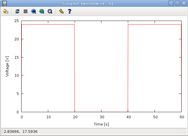
There's a result with Gnuplot :
With the right-click you can do a measure easily.
Q/A
To add input/output in gschem, some problems can arise. If the gnelist is not able to make the connection between the input label and the output label, it is because you have probably misconfigured your input/output element. For an optimal configuration, you need to edit the component attribut, add the net attribut and then enter the label name.
Example
Your input label is connected to PortB of your uC. Double click the input, add the net, and insert XXXX:1 (replace X by the correct name, e.g PORTB:1)
gschem2pcb with command line
gsch2pcb EdgeBoard_DS18B20.sch –elements-dir ../gEDA_library/PCB_elements/
